Google Nest Mini Teardown
Google Nest Mini Teardown
Because I am a Google Play Music member, I was recently offered a Google Nest Mini free of charge. I had little interest in Google’s in-home assistant since I already had both a Google Home Mini and an Amazon Echo (and I must say that I prefer Alexa to the Google Assistant, who lacks both humor and singing capacities).
Reading online, I was first amazed by how little hardware information was available for the Google Nest Mini, but most importantly, what was different from the previous iteration. Without further due, I dived in my own personal teardown of the Google Nest Mini.
TL;DR
- New thermals
- New Synaptics AS370 A1 for on-device voice inference
- More flash (256MB is now 4GB)
The torture teardown
The previous iteration had a fun little textured rubber circle that was glued to the bottom and hid the screws. Unfortunately, there was no such thing here, but there was a screw under a removable rubber pad that was easily accessible. After removing the screw, it was not immediately clear to me how to open it so I heated the bottom of the GNM with a heat gun. Turns out that was a very bad idea and the rubber cover came off deformed and unusable.
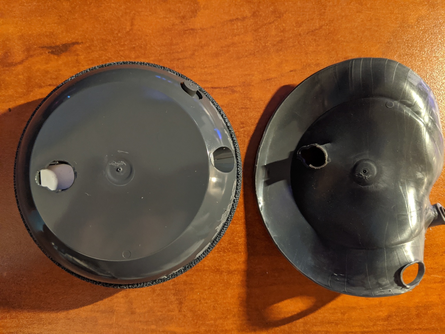
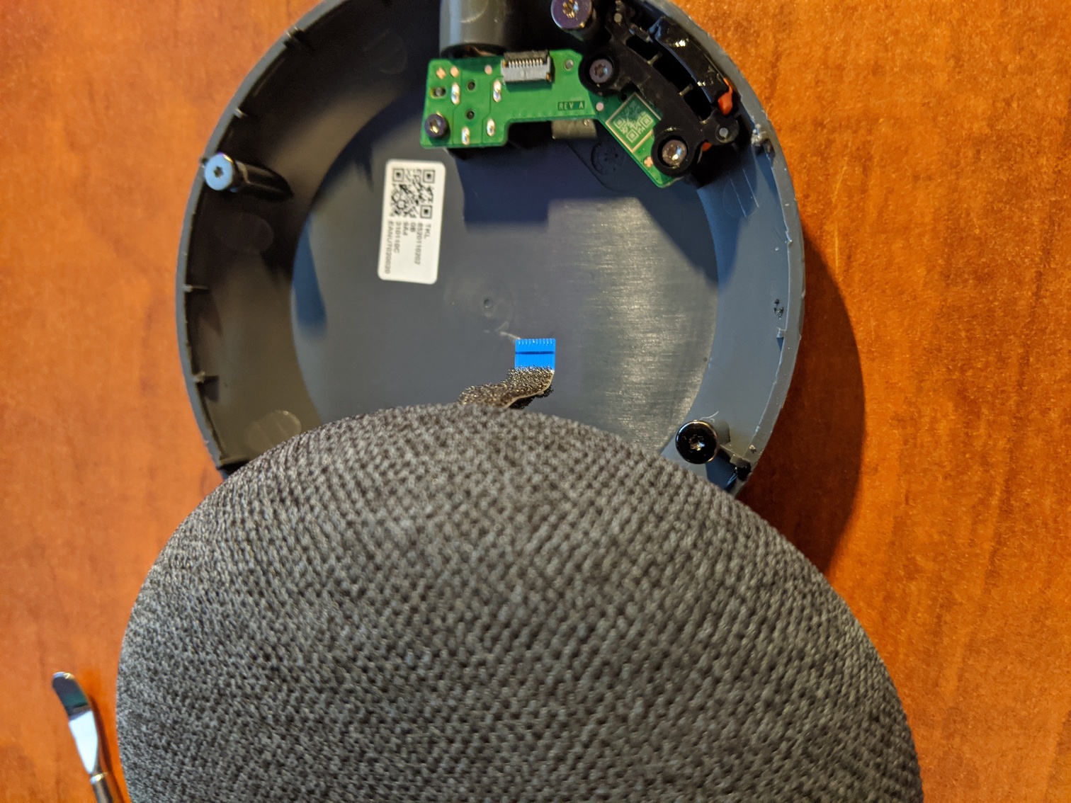
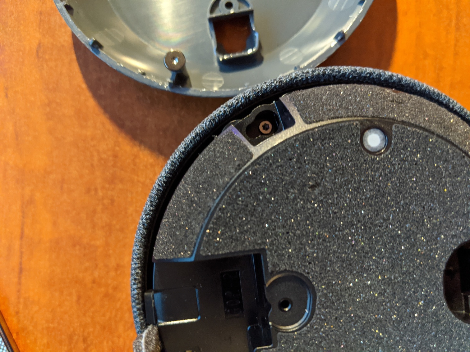
Playing with it for a while I noticed that it could be rotated and opened, revealing four T6 screws, which are attaching the speaker to the upper part. After carefully disconnecting said speaker, we are greeted with another set of five T6 screws.
Unscrewing those will reveal the board itself.
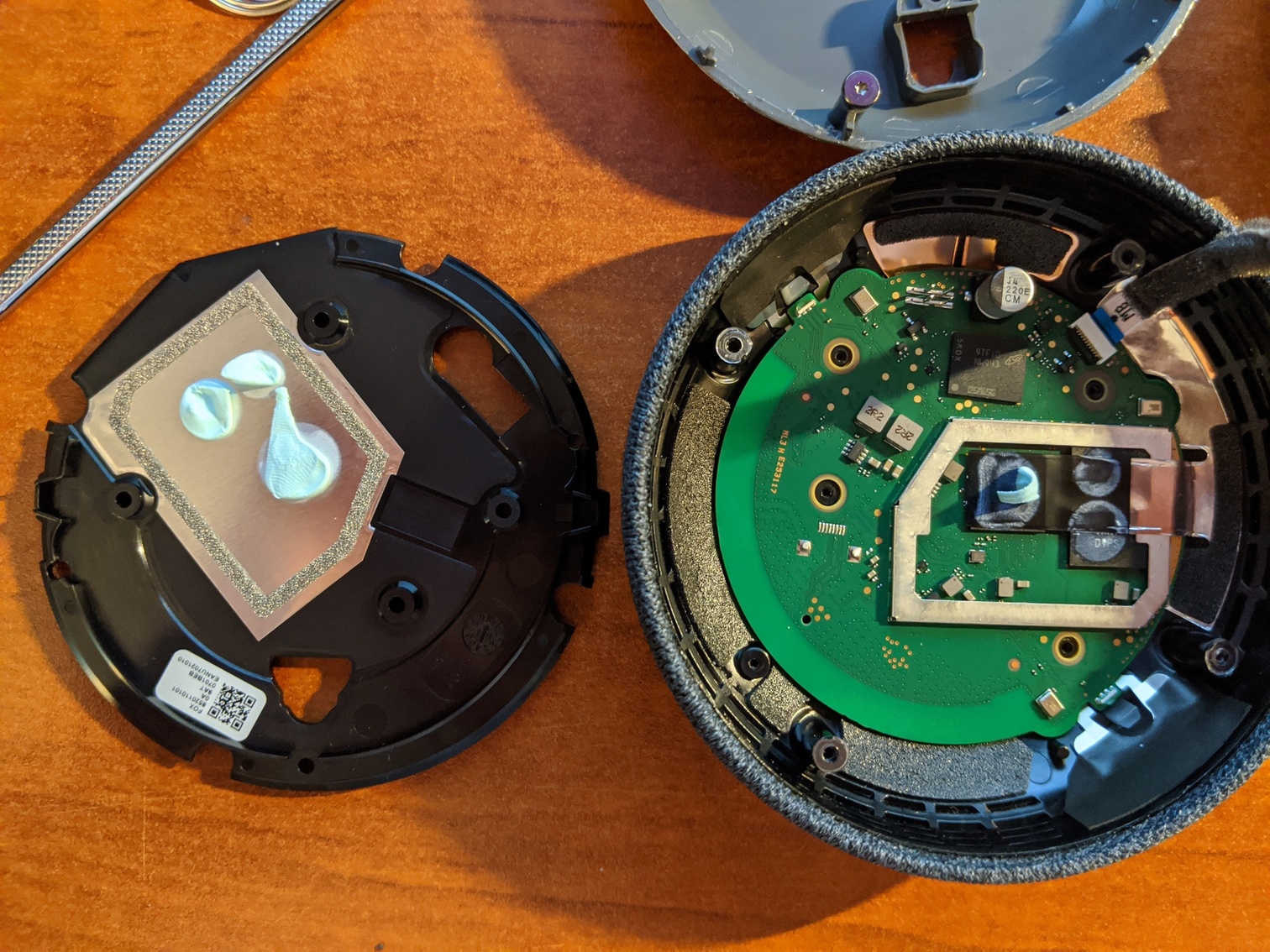
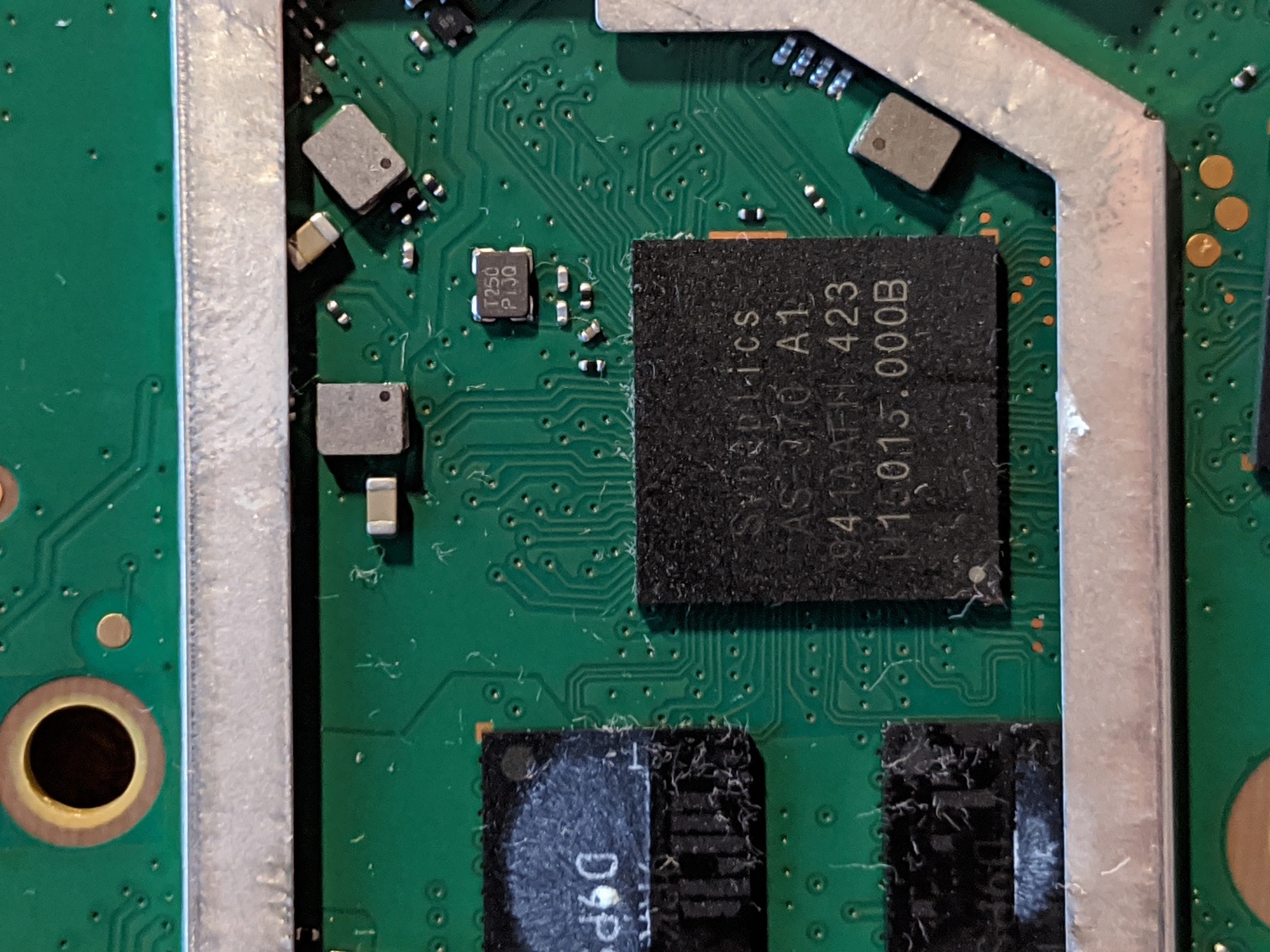
The first thing that we notice is the newly added thermal compound between the Synaptic chip and both of the DDR3-1866 modules, and it seems that some actual effort was put into dissipating the heat. Some back of the envelope calculations can shed some light on the reason why. The previous generation used a 5V@1.8A power supply, for a maximum TDP of 9W. The new generation on the other hand, uses a 14V@1.1A power supply which outputs no less than 15.4W, or about 70% more. With that in mind, one interesting difference is that the 1st generation device included an internal heatsink that was made of unknown metal (perhaps nickel?) while the new one boasts a full-plastic separator but with a more sophisticated heat management design.
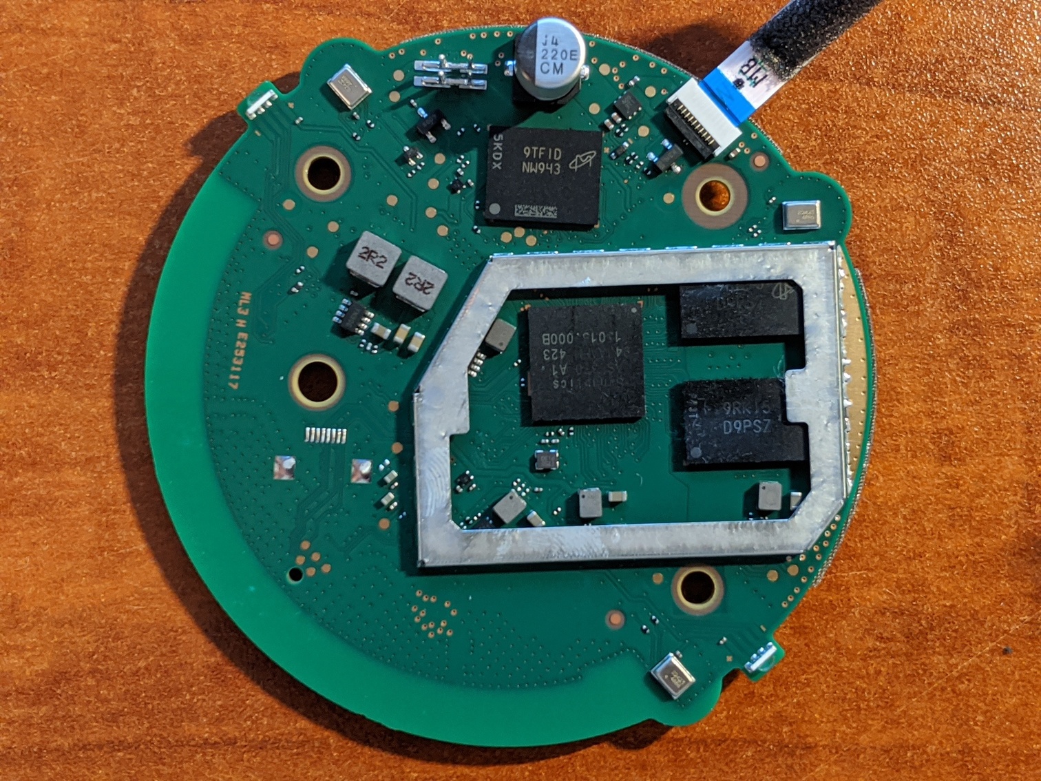
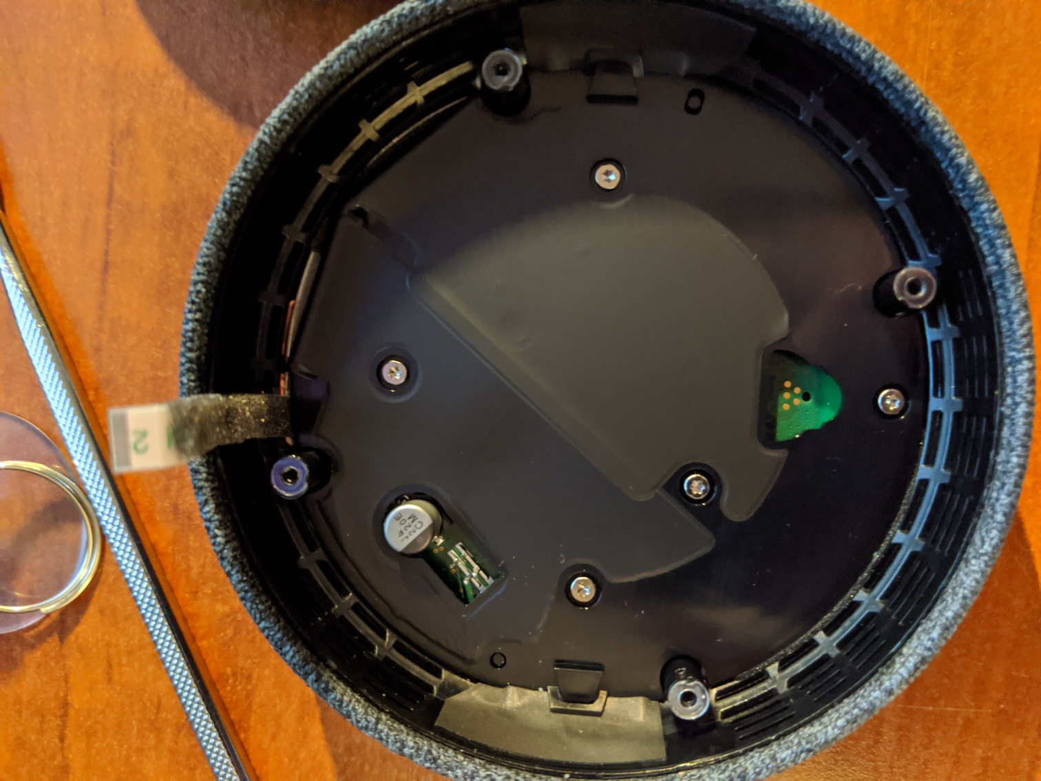
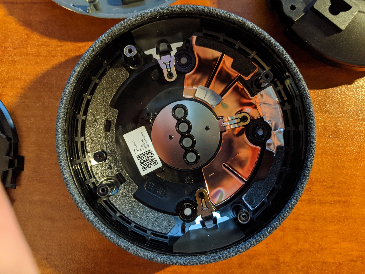
When we remove the board, we can see that little changed on the other side, with both microphones and four LEDs are in their old spot. The new microphone can be seen in the image.
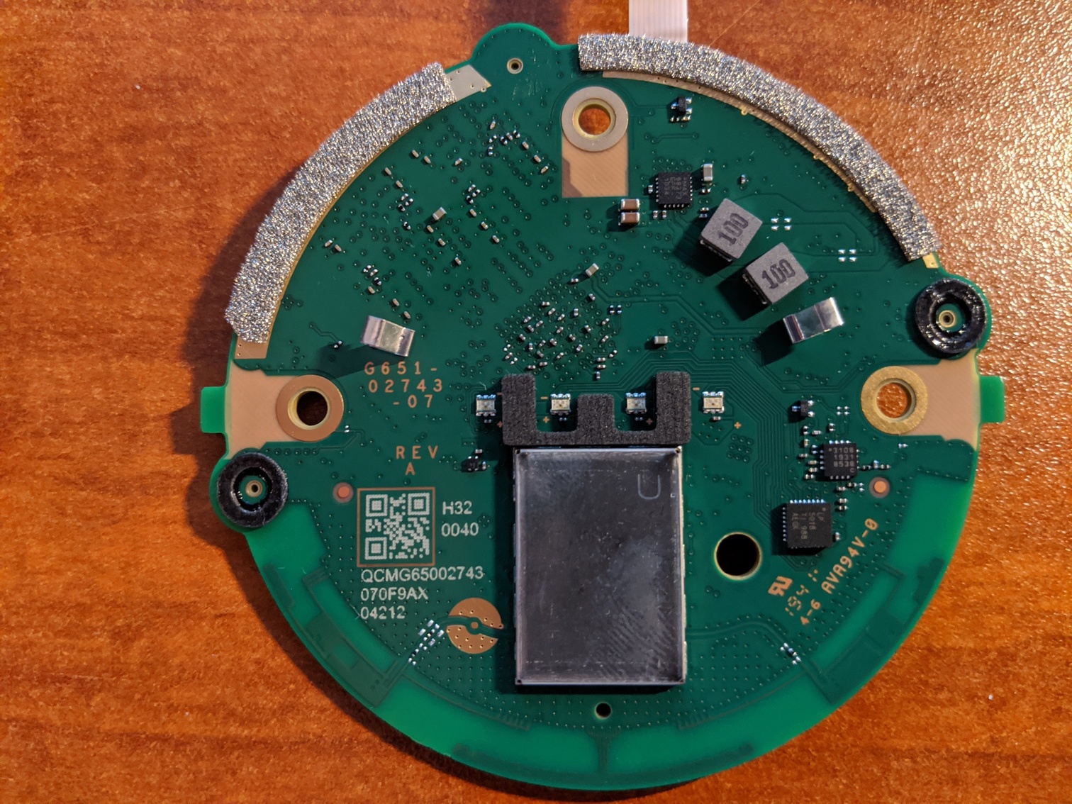
Unfortunately, the actual CPU is under a soldered protector/heatsinks, unlike the previous iteration that had removable ones. Since I do not own the proper tools to remove the metal shield, and wish to keep the device itself, I will rely on the official spec sheet which claims that it is a Quad-core 64-bit ARM CPU clocked at 1.4GHz which would be an upgrade over the dual-core processor boasted by the 1st generation.
And there ends the teardown, below you will find a more exhaustive hardware list. While I lack the skillset to properly reverse engineer and root the GNM, I hope that Google’s generosity will put it in the hands of more capable hackers because in its current form, it would be a more than capable Linux server with no less than 4GB of RAM, 4GB of flash memory and a quad-core processor.
The hardware
- 2x Micron DDR3-1866 2GB modules (specs)
- 1x Micron 4GB flash module (specs)
- 1x Synaptics AS370 A1 ML module (press release)
- 1x Unknown Quad-Core 64-bit ARM CPU
- 3x Far-fields microphones